Search results
Search for "spectroscopic ellipsometry" in Full Text gives 35 result(s) in Beilstein Journal of Nanotechnology.
CdSe/ZnS quantum dots as a booster in the active layer of distributed ternary organic photovoltaics
Beilstein J. Nanotechnol. 2024, 15, 144–156, doi:10.3762/bjnano.15.14

- spectra of a solid were studied as a thin film deposited on quartz, and measurements in solution were obtained in chloroform. The wavelength ranged from 250 to 1000 nm. A Woolam M-2000 ellipsometer was used for spectroscopic ellipsometry analysis. The measurement range was 350–1650 nm. The measurement was
- fluorophores emitting light signifies the occurrence of the quenching process. Spectroscopic ellipsometry Spectroscopic ellipsometry studies were performed to determine changes in optical performance with temperature. A multilayer model with a silicon substrate layer was fitted to the obtained Ψ and Δ values


In situ optical sub-wavelength thickness control of porous anodic aluminum oxide
Beilstein J. Nanotechnol. 2024, 15, 126–133, doi:10.3762/bjnano.15.12

- effective thickness below 300 nm could be produced with a few nanometers accuracy using single-crystal aluminum substrates. The results were confirmed using spectroscopic ellipsometry. The method for controlling the thickness during anodization eliminates the necessity of sample sectioning for electron
- achieve precise optical characterization, one could employ spectroscopic ellipsometry (SE) with more refined division into sub-layers [26] and consider additional material properties, such as the anisotropy of PAAO [27] and the optical dispersion of the refractive index (RI) of Al2O3 [28]. However, for
- anodization were confirmed using post-production spectroscopic ellipsometry, showing 1–2 nm variation (standard deviation) within each sample. The process is inherently non-invasive and eliminates the need for slicing the sample to measure thickness, as one might do with electron microscopy, for instance


Low temperature atomic layer deposition of cobalt using dicobalt hexacarbonyl-1-heptyne as precursor
Beilstein J. Nanotechnol. 2023, 14, 951–963, doi:10.3762/bjnano.14.78

- growth rate (blue diamonds) extracted by using a linear growth approximation. XPS measurements of the CVD film deposited at 150 °C. Growth per cycle of ALD processes with [Co2(CO)6HC≡CC5H11] precursor at various temperatures. Film thickness evolution measured by in line spectroscopic ellipsometry for a


Impact of device design on the electronic and optoelectronic properties of integrated Ru-terpyridine complexes
Beilstein J. Nanotechnol. 2022, 13, 219–229, doi:10.3762/bjnano.13.16

- was verified by infrared reflection absorption spectroscopy (IRRAS) and surface-enhanced Raman spectroscopy in combination with density functional theory calculations, as well as variable angle spectroscopic ellipsometry. Based on this wire formation protocol the on-chip preparation of Ru(TP)2-complex


Atomic layer deposited films of Al2O3 on fluorine-doped tin oxide electrodes: stability and barrier properties
Beilstein J. Nanotechnol. 2021, 12, 24–34, doi:10.3762/bjnano.12.2

- cycles. The layer thickness of the films was determined via referenced spectroscopic ellipsometry (RSE, Accurion). In the range of 10 to 200 deposition cycles, the measured deposition rate was 0.085 nm/cycle, corresponding to layer thickness values of 2.5, 5, 10, and 17 nm, respectively. For dissolution


Growth of lithium hydride thin films from solutions: Towards solution atomic layer deposition of lithiated films
Beilstein J. Nanotechnol. 2019, 10, 1443–1451, doi:10.3762/bjnano.10.142

- to be homogeneous and rough as seen in Figure 9. Cross-sectional SEM was performed to estimate the film thickness as a reference for spectroscopic ellipsometry (Figure 10). Based on the SEM image, a Cauchy model was created with a constant thickness of 45 nm while all other parameters were fitted
- the deposition and the high risk of contamination during long runs, only a few thick samples were prepared as cross sections. Spectroscopic ellipsometry measurements to determine the growth curve were performed directly after deposition (Figure 11). The deviations from the fit, RMSE = 0.65, in Figure
- crystalline when deposited at room temperature, making further post-processing unnecessary. The air sensitivity of this solid requires in situ materials characterization using methods such as spectroscopic ellipsometry, XPS and Auger spectroscopy. Further development of the process, especially more


On the transformation of “zincone”-like into porous ZnO thin films from sub-saturated plasma enhanced atomic layer deposition
Beilstein J. Nanotechnol. 2019, 10, 746–759, doi:10.3762/bjnano.10.74

- doses below self-limiting values. Nanoporous ZnO thin films were subsequently obtained by calcination of the zincone-like layers between 100–600 °C. Spectroscopic ellipsometry (SE) and X-ray diffraction (XRD) were adopted in situ during calcination to investigate the removal of carbon impurities
- fractions. The calcination of the hybrid layers was investigated in situ with spectroscopic ellipsometry (SE) and X-ray diffraction (XRD). Oxygen plasma was used as co-reactant together with diethylzinc (DEZ) in a room-temperature plasma-enhanced ALD process and, as a function of the plasma time exposure
- ]. Spectroscopic ellipsometry (J.A. Woollam M-2000V) was used to deter0mine the thickness and optical properties of the films after deposition. The measurements were carried out at three different angles (65°, 70°, and 75°) in a wavelength range from 370 to 1000 nm. The analysis of the spectra was performed with


Biocompatible organic–inorganic hybrid materials based on nucleobases and titanium developed by molecular layer deposition
Beilstein J. Nanotechnol. 2019, 10, 399–411, doi:10.3762/bjnano.10.39

- the middle of the adenine pulse stems from edge effects of the statistics. Film growth as a function of deposition temperature for TTIP and thymine (black squares), adenine (red circles), and uracil (blue triangles). (a) Refractive index at 632.8 nm as measured by spectroscopic ellipsometry and (b
- ) (b) uracil (225 °C, 122 nm) and (c) adenine (225 °C, 69 nm). Deposition conditions for QCM investigation and obtained pulse and purge parameters. Film thickness (nm) after 15 minutes, 3 hours and 4 days of exposure to water as measured by spectroscopic ellipsometry for Ti-thymine (at 225 °C), Ti
- -uracil (at 225 °C), Ti-adenine (at 250 °C). Refractive index at 632.8 nm as measured by spectroscopic ellipsometry and film density as measured by XRR before and after exposure to water for Ti-thymine (at 250 °C), Ti-uracil (at 225 °C), Ti-adenine (at 250 °C). Supporting Information Supporting


Geometrical optimisation of core–shell nanowire arrays for enhanced absorption in thin crystalline silicon heterojunction solar cells
Beilstein J. Nanotechnol. 2019, 10, 322–331, doi:10.3762/bjnano.10.31

- the flat c-Si substrates were characterised via spectroscopic ellipsometry. Finally, using physical vapour deposition, metal electrodes consisting of Ag/Cr/Al were deposited at the front (as patterned grids) and at the rear surfaces of the wafer (full area), with thickness values of 300/30/300 nm and


Site-controlled formation of single Si nanocrystals in a buried SiO2 matrix using ion beam mixing
Beilstein J. Nanotechnol. 2018, 9, 2883–2892, doi:10.3762/bjnano.9.267

- are based on p-doped Si wafers with a specific resistivity of 10 Ω cm. The buried SiO2 layer was grown via thermal oxidation at 1123 K in dry O2 atmosphere in a furnace followed by RF-sputtering of an amorphous Si layer. The thickness of the oxide layer was measured by spectroscopic ellipsometry in


A differential Hall effect measurement method with sub-nanometre resolution for active dopant concentration profiling in ultrathin doped Si1−xGex and Si layers
Beilstein J. Nanotechnol. 2018, 9, 1926–1939, doi:10.3762/bjnano.9.184

- including time, temperature and Ge content. For this, spectroscopic ellipsometry (with a HORIBA Jobin Yvon system) was used as a fast, reliable and non-destructive method for the measurement of the removed thickness. We developed an empirical model for the quantification of the SiGe thickness measurement


P3HT:PCBM blend films phase diagram on the base of variable-temperature spectroscopic ellipsometry
Beilstein J. Nanotechnol. 2018, 9, 1108–1115, doi:10.3762/bjnano.9.102

- composition of poly(3-hexylthiophene) (P3HT):[6,6]-phenyl-C61-butyric acid methyl ester (PCBM) blend films influences their phase transitions using variable-temperature spectroscopic ellipsometry. We demonstrate that this non-destructive method is a very sensitive optical technique to investigate the phase
- temperature changes. Characteristic temperatures determined from the slope changes of the Δ(T) plot appeared to be very good guess values for the phase transition temperatures. Keywords: non-linear optics; organic semiconductors; spectroscopic ellipsometry; theoretical modeling; thin films; Introduction The
- spectroscopic ellipsometry (SE). Moreover, with both techniques they detected two Tg transitions in thin films of P3HT:PCBM for a certain range of PCBM content. SE is a non-destructive and very sensitive technique for thin films investigations [23][24][25]. Generally, ellipsometry measures a change in the


Cyclodextrin inhibits zinc corrosion by destabilizing point defect formation in the oxide layer
Beilstein J. Nanotechnol. 2018, 9, 936–944, doi:10.3762/bjnano.9.86
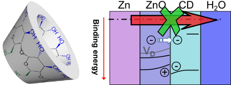
- the EIS measurements a quantitative comparison of the efficiencies is not reasonable. In situ spectroscopic ellipsometry experiments conducted both in 0.1 M KCl as well as in 0.1 M KCl with 5.3 mM β-CD show no formation of an adsorbate layer on the samples (Supporting Information File 1, Figure S6
- microscope. The samples were irradiated with an excitation wavelength of 532.1 nm/2.33 eV through a microscope objective of 100× magnification and with a numerical aperture of 0.75. In situ spectroscopic ellipsometry (SE) was performed on Zn samples polished down to a 1 μm diamond suspension. Experiments
- measurements, detailed peak decomposition of ADXPS data, Raman spectra, and in situ spectroscopic ellipsometry data. Acknowledgements M. K. acknowledges the Silesian University of Technology’s rector pro-quality grant no. 14/990/RGJ17/0076. Prof. M. Stratmann is acknowledged for continuous support.


Growth model and structure evolution of Ag layers deposited on Ge films
Beilstein J. Nanotechnol. 2018, 9, 66–76, doi:10.3762/bjnano.9.9

- thick Ag films deposited on 2 nm thick Ge wetting layer and capped with 3 nm thick LiF overlayer, measured using spectroscopic ellipsometry 10 days after the deposition process. The black and red curves have been reproduced from [4]. Transmission spectra of non-annealed (left column) and annealed (right
- ) Transmission spectra of Ge/Ag multilayer structure with total thickness of 20 nm. (b) Imaginary part of permittivity for 20 nm thick silver film deposited on 2 nm thick Ge wetting layer, measured using spectroscopic ellipsometry at 1, 10 and 60 days after deposition (solid lines), as well as Maxwell–Garnett


Expanding the molecular-ruler process through vapor deposition of hexadecanethiol
Beilstein J. Nanotechnol. 2017, 8, 2339–2344, doi:10.3762/bjnano.8.233

- lowest-intensity region between the two Au regions corresponds to the nanogap where the Si substrate is exposed. This nanogap measures 26.0 ± 4.3 nm and is consistent with the thickness of the Cu-ligated MHDA decalayer measured via spectroscopic ellipsometry (24.8 ± 0.1 nm) and the thickness of Cu
- capping (31.0 ± 1.0 nm) measured via spectroscopic ellipsometry. The standard deviations of the nanogap widths, thus the quality of the nanogaps, result from the morphologies of the Cu-ligated multilayers of MHDA only and MHDA with vapor-phase deposition of C16 (Figure S2, Supporting Information File 1


(Metallo)porphyrins for potential materials science applications
Beilstein J. Nanotechnol. 2017, 8, 1786–1800, doi:10.3762/bjnano.8.180

- covered with 100 nm thick Au layers were applied. Variable angle spectroscopic ellipsometry (VASE) was used to determine the absorption spectra of the as-obtained thin films. The extinction coefficients of the thin films display the typical features expected for (metallo)porphyrins, including expected
- corresponding to the observed features in the absorption spectra. This indicates that the LUMO of these molecules generating the Q band is a formerly degenerated state undergoing Zeeman splitting in the magnetic field. With respect to the spectroscopic ellipsometry and magneto-optical Kerr effect spectroscopy


Charge transfer from and to manganese phthalocyanine: bulk materials and interfaces
Beilstein J. Nanotechnol. 2017, 8, 1601–1615, doi:10.3762/bjnano.8.160

- photoemission spectroscopy (IPES), electron energy-loss spectroscopy (EELS), spectroscopic ellipsometry and X-ray absorption spectroscopy (XAS). Here, we only briefly mention the kind of information that is provided by these methods, and we refer the reader to comprehensive literature for detailed information
- moment of open shells is accessible. Spectroscopic ellipsometry [47][48][49] measures the change in the light polarization after reflection on a sample surface. This information allows for the determination of the real and the imaginary part of the dielectric function. XAS [42][50] is equivalent to EELS
- were determined using EELS and spectroscopic ellipsometry. In Figure 2 we show the corresponding results. The EELS measurements were carried out at a momentum transfer of 0.1 Å−1 which represents the so-called optical limit, i.e., the data are equivalent to those from corresponding optical studies [43


Deposition of exchange-coupled dinickel complexes on gold substrates utilizing ambidentate mercapto-carboxylato ligands
Beilstein J. Nanotechnol. 2017, 8, 1375–1387, doi:10.3762/bjnano.8.139

- ) and 8 (J = +20.8 cm−1; H = −2JS1S2). The reactivity of complexes 6–8 is reminiscent of that of pure thiolato ligands, which readily chemisorb on Au surfaces as verified by contact angle, atomic force microscopy (AFM) and spectroscopic ellipsometry measurements. The large [Ni2L] tail groups, however
- “auration” of 2 and 3 with AuI sources leads to the trinuclear NiII2AuI species 4 and 5. Moreover, complexes 2 and 3 interact also with Au surfaces via Au–S and Au–P bonds without complex disintegration as established by contact angle, spectroscopic ellipsometry, atomic force microscopy (AFM), X-ray
- ). The crystal structure, reactivity features, and magnetic properties of compounds 6–8 are presented along with the results stemming from characterization of the surface assemblies by contact angle measurements, spectroscopic ellipsometry, AFM and transport measurements. To our knowledge, polynuclear


Optical response of heterogeneous polymer layers containing silver nanostructures
Beilstein J. Nanotechnol. 2017, 8, 1065–1072, doi:10.3762/bjnano.8.108

- colloidal solutions range from 390 to 1300 nm. The non-absorbing, transparent polymer matrix poly(vinylpyrrolidone) (PVP) was chosen because of its suitable optical and chemical properties. The optical studies of the layers include spectrophotometry and spectroscopic ellipsometry measurements, which provide
- the nanoparticles to complete the optical characterization. A simple analysis method is proposed to obtain the complex refractive index of nanospheres and nanoprisms in a polymer matrix. Keywords: nanoprisms; nanospheres; plasmonic nanoparticles; spectroscopic ellipsometry; thin film layers
- with computer simulations and transmission electron microscopy (TEM) imaging. Spectrophotometer and spectroscopic ellipsometry measurements of the PVP host matrix validated its non-absorbing and transparent properties. Spectroscopic ellipsometry measurements of the heterogeneous layers of nanospheres


Vapor-phase-synthesized fluoroacrylate polymer thin films: thermal stability and structural properties
Beilstein J. Nanotechnol. 2017, 8, 933–942, doi:10.3762/bjnano.8.95

- . Keywords: EGDMA; iCVD; in situ; PFDA; spectroscopic ellipsometry; temperature dependent; X-ray diffraction; Introduction Fluoropolymers, such as polytetrafluoroethylene, are interesting for a variety of different applications due to their low surface energy. The resultant hydrophobic and oleophobic
- situ temperature-dependent spectroscopic ellipsometry measurements were performed on a Woollam M-2000 ellipsometer (J.A. Woollam Co., USA), equipped with a THMS600 temperature stage (Linkam, UK) under nitrogen atmosphere. The samples were investigated in the temperature range between 10 and 150 °C at a
- the amorphous, cross-linked p-(PFDA-co-EGDMA) films, in situ spectroscopic ellipsometry was utilized. In Figure 6, the evolution of the film thickness (normalized to the thickness at 25 °C) is depicted as a function of temperature, as determined from ellipsometry data. After several equilibration


Thin SnOx films for surface plasmon resonance enhanced ellipsometric gas sensing (SPREE)
Beilstein J. Nanotechnol. 2017, 8, 522–529, doi:10.3762/bjnano.8.56

- was used. The Fe-doped SnOx was deposited with a 20%/80% oxygen/argon mixture with a pressure of 0.2 Pa. The thickness of the SnOx and Fe:SnOx overcoatings was 7 nm and 5 nm, respectively. The thickness was determined by using spectroscopic ellipsometry. The layer morphology was also determined by


Advances in the fabrication of graphene transistors on flexible substrates
Beilstein J. Nanotechnol. 2017, 8, 467–474, doi:10.3762/bjnano.8.50

- collected by tapping mode atomic force microscopy (tAFM) for the LT growth (Figure 1a left) is comparable to the morphology obtained by the ST growth (Figure 1a right). The dielectric thickness and the consequent growth per cycle was determined by spectroscopic ellipsometry measurements performed on an


Precise in situ etch depth control of multilayered III−V semiconductor samples with reflectance anisotropy spectroscopy (RAS) equipment
Beilstein J. Nanotechnol. 2016, 7, 1783–1793, doi:10.3762/bjnano.7.171

- . Those are mostly optical, for instance (laser) interferometry and reflectometry [16][17] or (spectroscopic) ellipsometry [18]. Also, combinations of several techniques are applied [19][20][21]. RAS incorporates some advantages. Usually for RAS reflectometric information is recorded for a broad spectral


An ellipsometric approach towards the description of inhomogeneous polymer-based Langmuir layers
Beilstein J. Nanotechnol. 2016, 7, 1156–1165, doi:10.3762/bjnano.7.107

- enabled and morphological inhomogeneity could be quantified. Keywords: ellipsometric mapping; Langmuir monolayer; polyester; root mean square roughness; spectroscopic ellipsometry; Introduction Ellipsometry is an established in situ technique to investigate surfaces, capable to derive information about
- work, the basic principles of ellipsometry have not changed, but its measurement modes have expanded. The main developments of ellipsometry are represented by spectroscopic ellipsometry (SE) and various angles spectroscopic ellipsometry (VASE), all of them developed to improve the performance of
- pronounced structuration. Additionally, the demonstration of spectroscopic ellipsometry on PPDL-based Langmuir layers has already been shown [17]. Morphological transitions that lead to inhomogeneous structures can be caused by a plethora of compounds at the air–water interface and are known for fatty acid


Manufacturing and investigation of physical properties of polyacrylonitrile nanofibre composites with SiO2, TiO2 and Bi2O3 nanoparticles
Beilstein J. Nanotechnol. 2016, 7, 1141–1155, doi:10.3762/bjnano.7.106

- concentration by weight of the used reinforcing phase, which was as follows: 0%, 4%, 8% and 12% for each type of nanoparticles. The width of the band gap was determined on the basis of the absorption spectra of radiation (UV–vis) and ellipsometry methods. Spectroscopic ellipsometry has been used in order to
- determine the dielectric constant, refractive index and the thickness of the obtained fibrous mats. Keywords: ceramic nanoparticles; electrospinning methods; polyacrylonitrile; polymer composite nanofibres; spectroscopic ellipsometry; Introduction Over the last decade, there has been a noticeable


